APPLICATION
Electronics & PCB Dispensing
Underfill, component staking, thermal materials, connector sealing, gasketing and potting across PCB and electronic assembly.
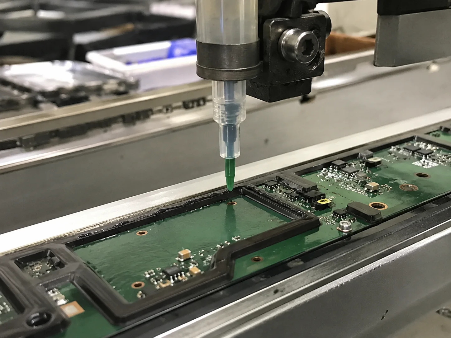
Underfill, component staking, thermal materials, connector sealing, gasketing and potting across PCB and electronic assembly.
The dominant process changes by product. These six patterns cover the most common engineering needs in this sector.
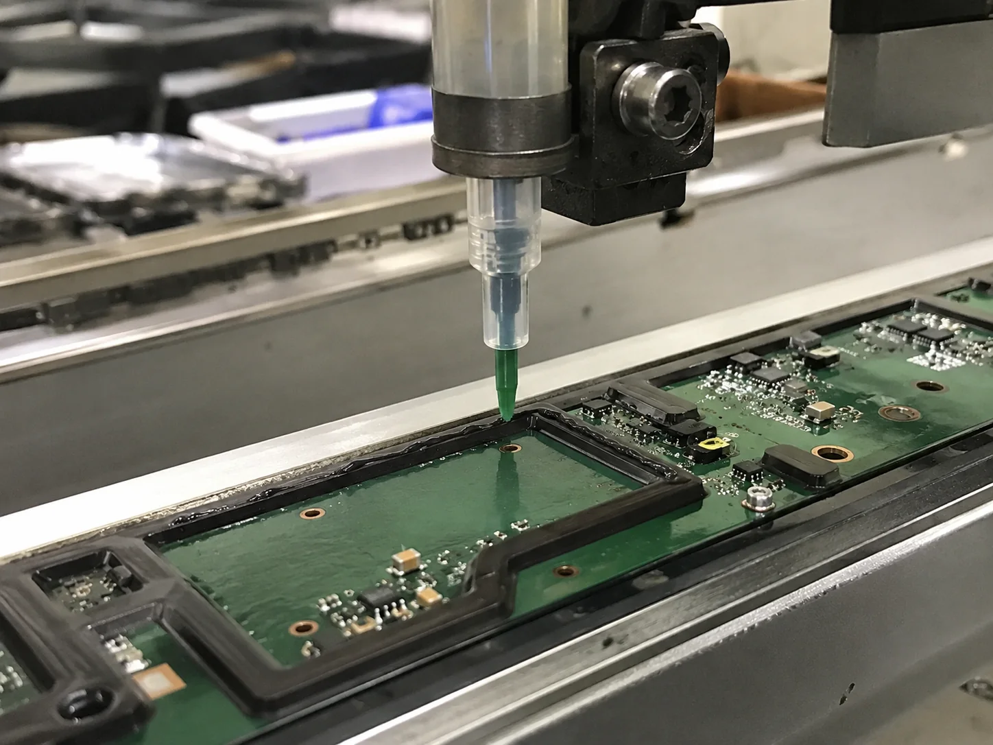
Control small dots and narrow beads while minimizing overflow and contamination.
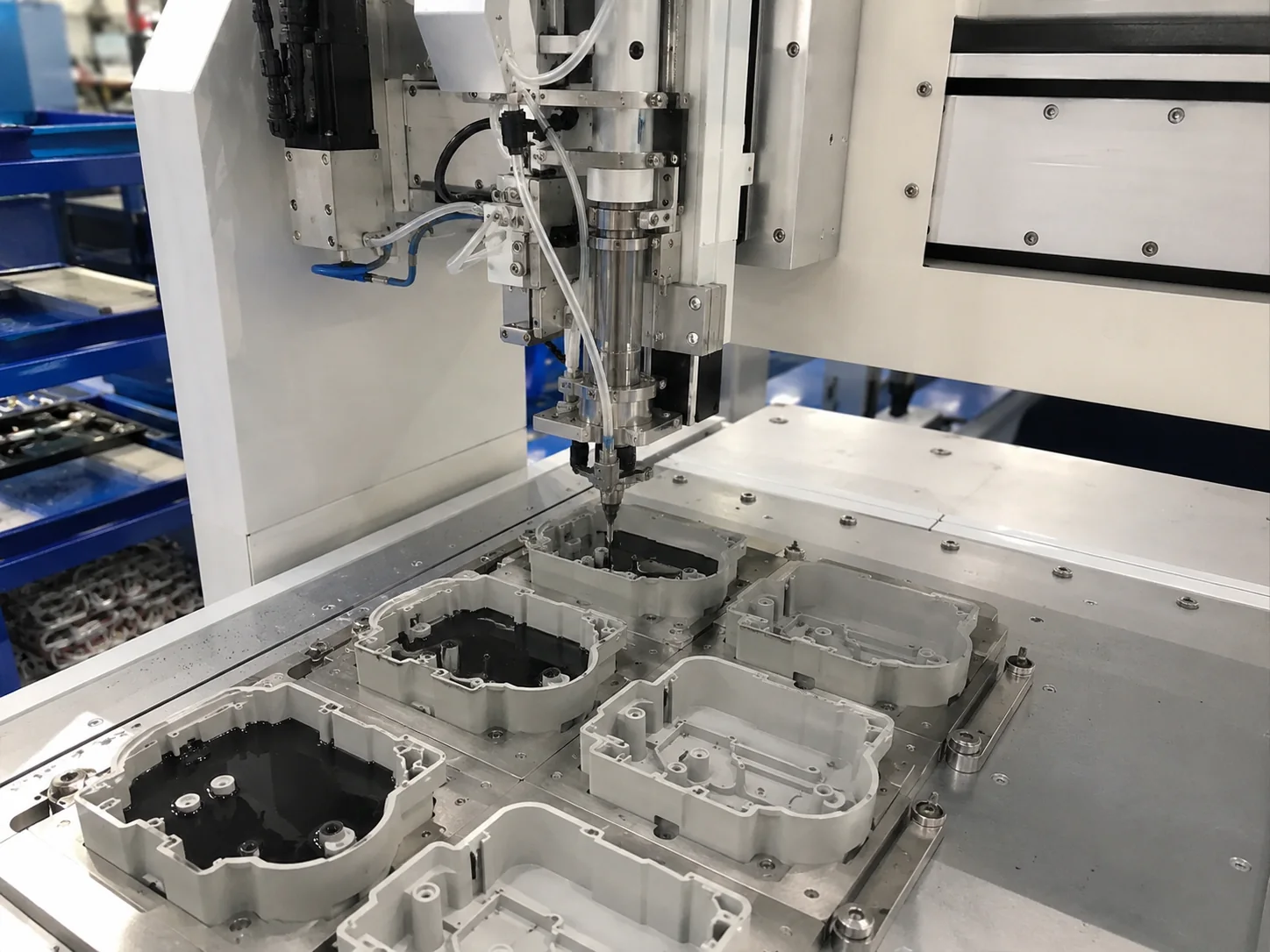
Balance gap, flow rate and shot volume to improve fill consistency and reduce void risk.
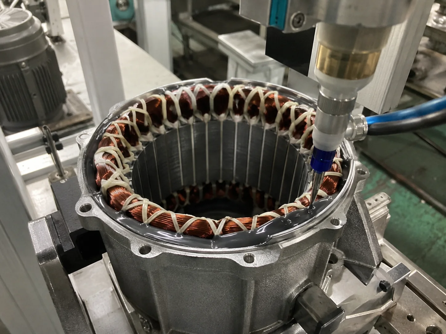
Dispense thermal gel, gap filler or adhesive with controlled coverage and bondline thickness.
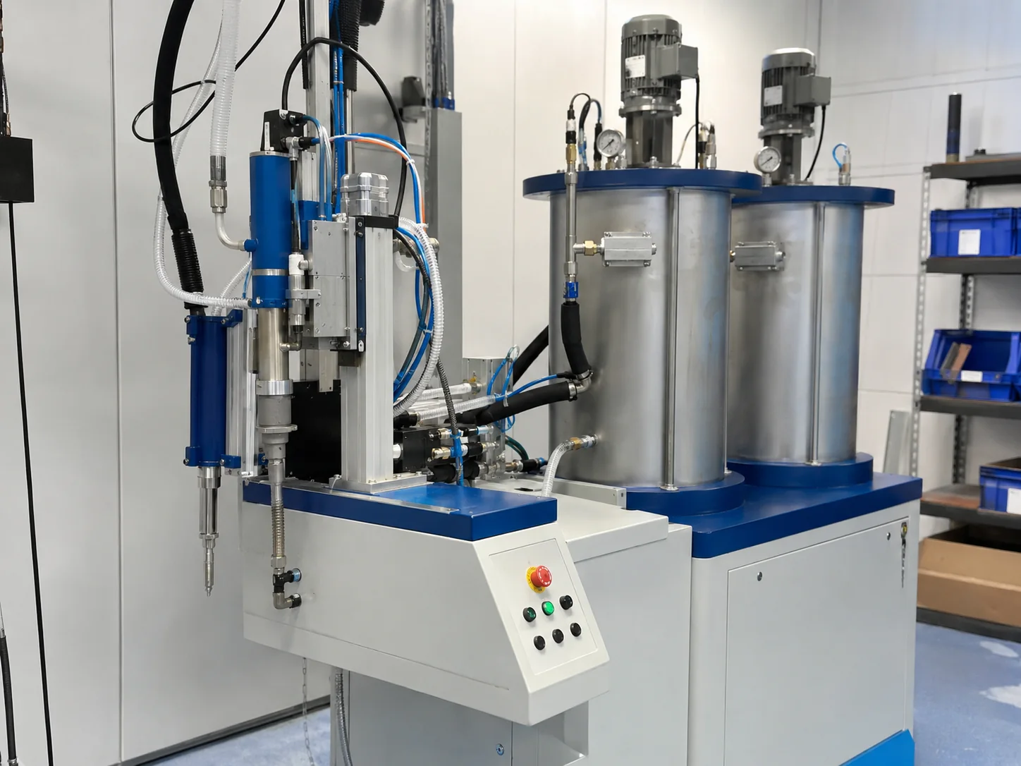
Apply continuous seals around connectors, housings and moisture-sensitive areas.
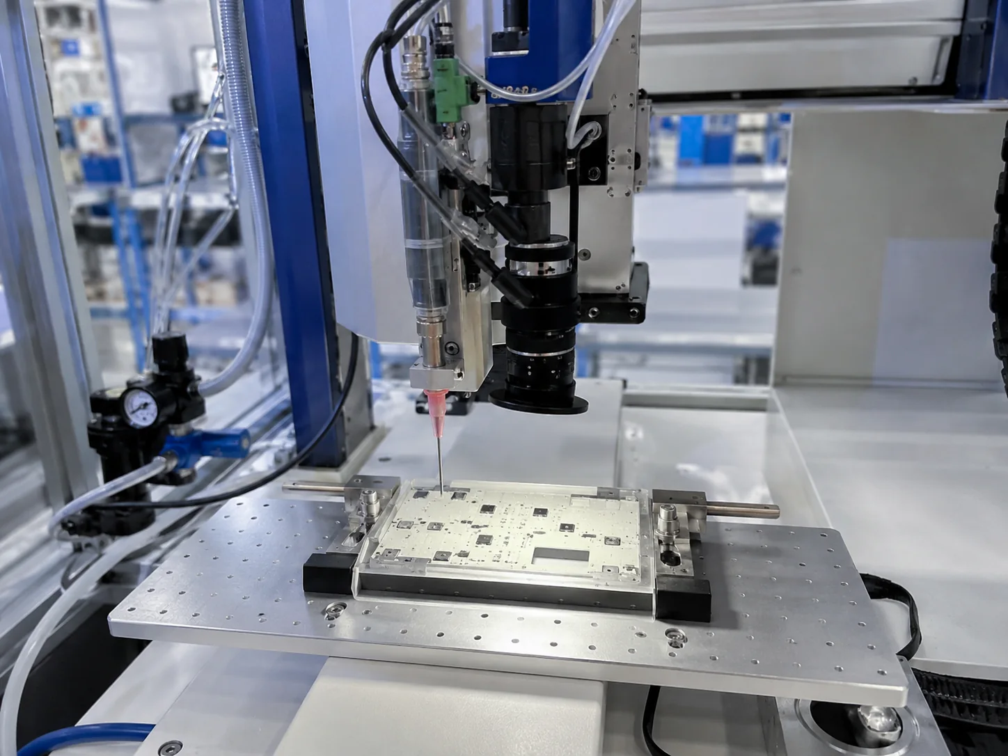
Use fiducials, edges or features to compensate PCB and fixture variation.
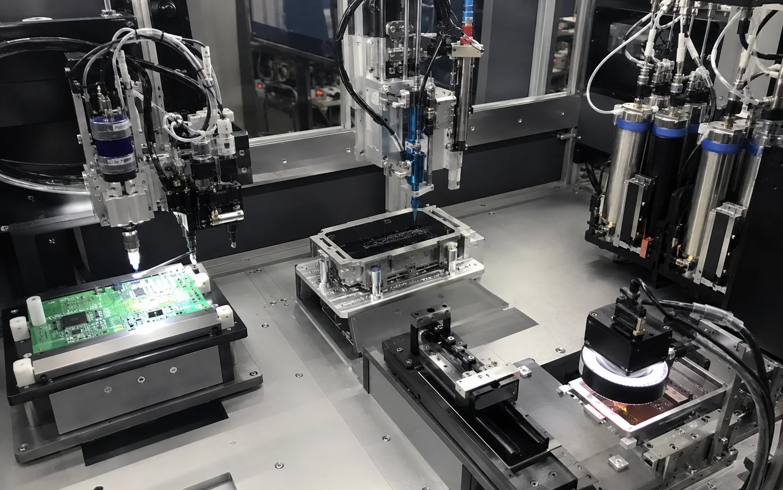
Connect conveyors, PLC and MES for recipe handling, traceability and automatic loading.
Confirm minimum dot or bead size, component clearance, PCB flatness, adhesive viscosity and cure method. High-mix lines may also require vision alignment, fixture changeover and recipe management.